Nvidia mandates TSMC 3nm base dies for all NVHBM suppliers
Nvidia requires Samsung, SK Hynix, and Micron to use TSMC’s 3nm process for NVHBM base dies to ensure consistency and reduce validation overhead.
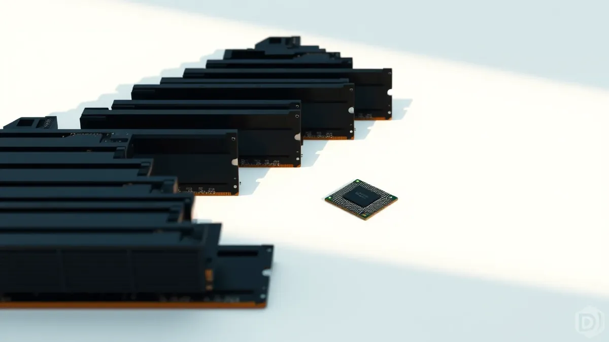
Key points
- Nvidia requires all three NVHBM suppliers to manufacture base dies using TSMC’s 3-nanometer process.
- Samsung will abandon its traditional turnkey approach for Nvidia chips, marking the first collaboration on HBM base dies.
- The shift aims to standardize performance across suppliers and reduce separate validation efforts for Nvidia.
Nvidia has instructed all three of its high-bandwidth memory suppliers to manufacture base dies using TSMC’s 3-nanometer process, according to a report by The Next Web citing Seoul Economic Daily. This directive affects Samsung Electronics, SK Hynix, and Micron, requiring them to align their production methods for Nvidia’s custom NVHBM chips.
The move represents a significant shift for Samsung, which previously used a turnkey approach that included manufacturing both the base die and the memory dies for its HBM products. According to the report, Samsung’s Device Solutions division agreed to this change after an internal review. It marks the first time Samsung and TSMC have collaborated on producing high-bandwidth memory components.
Strategic Rationale and Technical Changes
Nvidia seeks consistency across its supply chain, as different manufacturing methods can cause performance variations that are difficult to manage. By standardizing on TSMC’s 3nm process, Nvidia avoids the need to validate each supplier’s chips separately. Additionally, Nvidia requires the memory dies to be standardized on 1c, the sixth generation of DRAM technology, while the overall NVHBM design follows the seventh-generation HBM4E architecture.
NVHBM architecture relocates the memory controller from the GPU to the base die, freeing up space on the graphics processor for additional computing circuits. This design allows the physical layer communicating with other chips to be 60% smaller than in standard HBM. The result is up to 30% more bandwidth and 15% less power consumption compared to standard HBM4E.
Supply Chain and Market Context
The industry estimates TSMC’s 3nm yield at more than 90%, significantly higher than the approximately 60% yield for Samsung Foundry’s comparable 2nm process, SF2. TSMC is adding two 3nm production lines at Fab 18 in Tainan, with mass production scheduled for the first half of 2027 and 2028. Additional 3nm lines are planned for facilities in Arizona and Kumamoto, Japan.
UBS projects global HBM demand to reach 61.5 billion gigabits next year, a 91% increase, while new shipments are expected to total only 54.6 billion gigabits. This creates an anticipated shortfall of about 10%. As Threat Times reported on October 18, 2026, Samsung had already agreed to make Nvidia NVHBM base dies on TSMC’s 3nm process, confirming this broader strategic shift.
Samsung will continue using its turnkey approach for standard HBM4 and HBM4E products, which utilize its own 4nm base dies. The company will also maintain this method for custom HBM supplied to other customers, including AMD. The two companies previously collaborated four years ago when Samsung ensured its HBM fit TSMC’s packaging process.
What should you do?
Monitor supply chain announcements from major semiconductor vendors for updates on manufacturing process shifts. Track yield rates and production timelines for advanced nodes like TSMC’s 3nm, as these impact component availability. Review internal hardware roadmaps to assess potential delays or changes in performance characteristics for systems relying on next-generation memory.
What to do and how to stay safe: Nvidia
- Monitor official announcements from Nvidia and its memory suppliers regarding manufacturing process changes and product availability.
- Review hardware procurement timelines to account for potential shifts in production yields and supply chain constraints.
- Track industry reports on HBM demand versus supply to anticipate market volatility and pricing trends.
- Evaluate system architecture dependencies on specific memory technologies to prepare for architectural changes in future chips.
Step-by-step guide: Mobile Device Security: How to Protect Data Beyond Passwords
General security guidance from the Threat Times newsroom. It is not confirmed advice from the organisations named in this story.
Frequently asked questions
Why is Nvidia requiring suppliers to use TSMC's process?
Nvidia wants to ensure consistency in chip performance across suppliers and reduce the need to validate each supplier's chips separately.
Does this change apply to all of Samsung's HBM products?
No, Samsung will keep its turnkey approach for standard HBM4, HBM4E, and custom HBM for other customers like AMD.
What are the performance benefits of NVHBM?
NVHBM offers up to 30% more bandwidth and 15% less power consumption compared to standard HBM4E.